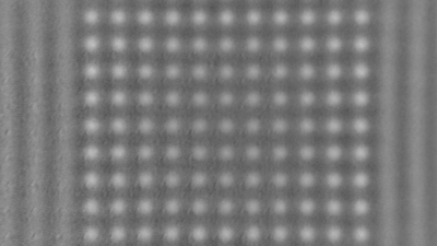
缺陷检测 Defect Inspection
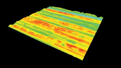
Deep saw marks detection on solar wafers
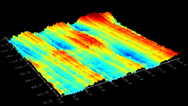
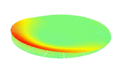
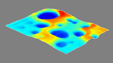
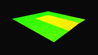
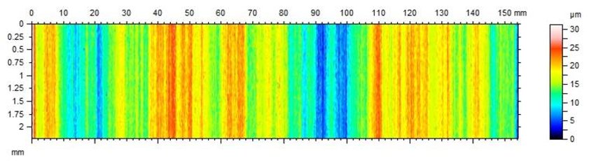
Silicon ingots are sliced into wafers using diamond wires. Small deviation of these wires during the sawing process may results in relatively deep marks that make the wafer fragile. This application describes such defect inspection on solar wafers.
Speed is a key requirement for this application, and the unrivaled acquisition speed of DHM® is a necessity:
- High throughput: 1 wafer per second !
- Measurements performed on a rubber band convey tray, without stopping the samples.
- Presence of vibrations due to surrounding of production facilities.
Description
Sample
- Wafer size: 150 x150 mm
- Inspected area: 150 x 5 mm
- Typical Depth Threshold: 10 micrometers
Conveyor
- Speed: 214 mm/s
- Height variation: < 300 μm
- Inspection time for each wafer: 0.7 second
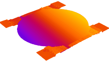
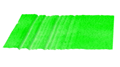
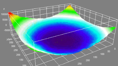
Results
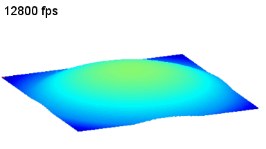
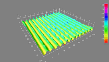
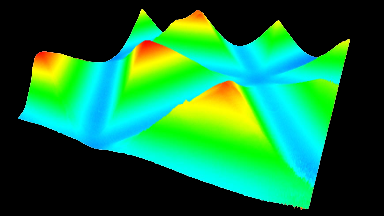
- 3D Measurement of a 150 mm x 2mm rough surface at a rate of 1 wafer per second
- Saw marks detection on the entire 3D surface measured
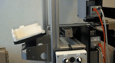
Instrument
- 2 OEM reflection DHM® heads:
- top and bottom surface inspection
- synthetic wavelength of 58.6 μm. Solar wafers have a rough surface that produces speckle. This specific optical configuration allows DHM® to extract precise profile cut.
- Size: 430 x 230 x 60 mm
- Weight: 10kg
- Magnification: 1.25
Automated Process
- Measurement start: triggered by an optical barrier
- Acquisition and stitching: 50 3D measurements in less than 1 second
- Decision Go/NoGo: based on topography measurement analysis
- Software: Dedicated acquisition and analysis software based on the Software Development Kit
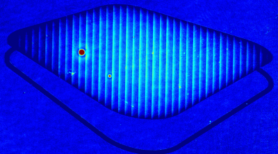
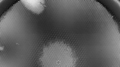
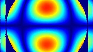
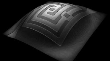
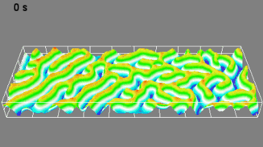
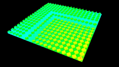
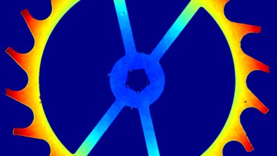
Automated Defect detection over the complete sphere surface
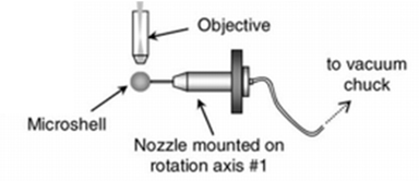
This application demonstrates automated defects detection over the entire surface of a semi-transparent microshell. The sample is hold by a small vacuum nozzle. Two rotation axes allow to cover its entire surface. Defects are detected and their geometrical characteristics measured. DHM® has been chosen among other techniques for this application considering:
- Manipulation complexity: sample wobbles if the rotation center and the sample center do not coincide
- Automated re-centering and focalization to compensate for the inevitable wobble
- Fast image stitching on a curved surface
- Need for short acquisition time
Challenges :
- Manipulation complexity: sample wobbles if the rotation axis does not the cross sample center
- Automated focalization to compensate wobble issue
- Fast image stitching on a curved surface
- For this project, alternative methods have been excluded due to their slow scanning process
Material and methods
Microscope
- DHM® R1000
- Motorized stage XYZ
- Two customized rotation axes
- Vacuum chuck to handle the sample with 2 small nozzles
Software
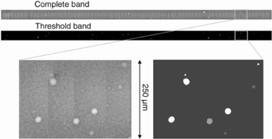
- Fast and automated stitching and digital curvature compensation enable the extraction of data along a band
- Automated focalization and coherence search are done at each step to acquire data with an optimal optical quality
- Remote TCP/IP to control DHM®
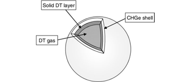
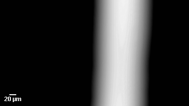
Microshells sample
- Material : CHGe sphere with an external solid layer made of deutriumtritium (D-T)
- Diameter : 0.8 mm
Results
- Bump detection over the complete sample surface, link to publication